
The Hidden Hardware Layer Inside Every Smart Device
By Space Coast Daily // September 22, 2026
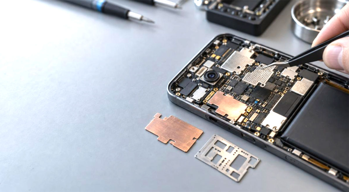
Open up any smart device and the parts that get the attention are obvious. The processor, the camera, the screen, the battery. They are what the marketing talks about and what the teardown videos zoom in on. Sitting quietly around all of them is another layer that almost nobody names, a set of small, precisely made metal parts that do the unglamorous work of holding everything together, moving heat, blocking interference, and letting each chip do its job. You never see them, and the device does not work without them.
This hidden layer is easy to dismiss because the parts look trivial. A thin sheet of metal with some holes in it. A little frame. A stamped-looking shield. But the performance of the expensive chip above them often depends on how well these quiet parts were made, and as devices shrink and chips run harder, that dependence is growing rather than shrinking.
The parts you never think about
Consider what is actually in the gap between the impressive components.
There is heat to deal with. A modern processor concentrates a lot of power into a tiny area, and the first thing that heat meets is a thin metal part, a spreader or a thermal layer, that has to pull it off the chip and pass it to whatever cools the device. If that part is not flat and clean, the heat does not move well, and the chip throttles no matter how fast it could theoretically run.
There is interference to contain. Radios, high-speed signals, and dense boards all leak electromagnetic noise, and thin metal shielding parts fence that noise in while often venting heat through fine openings at the same time. A phone that holds a clean signal in a crowded band owes part of that to shielding you will never see.
There is the matter of building the board at all. Before a single component is placed, solder paste is printed onto the board through a thin metal stencil whose openings decide how much paste lands where. Get that stencil wrong and the joints starve or bridge, and the finished board fails in ways that look like a chip problem but started at a piece of foil.
And there is testing. Before chips ship, they are checked on precision carriers, sockets, and probe tooling that hold them and make contact with contacts finer than a hair. That tooling is precision metalwork too, and it decides whether a good chip is correctly judged as good.
Around all of that sit connectors, lead frames that carry signals out of a chip package, filters and fine meshes, precise slits and apertures in optical parts, and the speaker grilles that let sound out while keeping dust and fingers away. None of these is the star of the device. Every one of them can ruin it.
Why a small part can cap a big chip
The reason this layer matters more than its size suggests is that it sits in the path of everything the expensive parts are trying to do.
A spreader that is warped leaves a gap, and a gap chokes the heat trying to escape. A stencil aperture that is off by a little prints the wrong amount of paste, and a weak joint fails later in the field. A burr on a shielding part scratches a coating or fouls a mating surface. A test carrier that is out of position reads a good die as bad. In each case the flaw is measured in microns, invisible to the eye, and its effect lands on a component worth many times more. The chip can only perform as well as the quiet metal around it allows, which is why the people who design demanding hardware care a great deal about parts that never appear in a spec sheet.
Why the hidden layer keeps getting harder
This work was never trivial, and it is getting harder for a simple reason. Devices keep getting smaller and denser while the chips inside them run hotter and faster, and both trends push straight onto the metal layer.
Smaller devices mean these parts have to be thinner and fit into tighter spaces, and thin metal is harder to keep flat and precise. Denser boards mean finer features, from micro-perforated shielding to closely spaced stencil apertures to the tiny holes in a filter or a heat-dissipation part. Those fine holes are their own manufacturing challenge, since a dense array of openings finer than the sheet is thick calls for precision micro-hole drilling rather than a stamping die, and every one of them has to be clean and consistent. Hotter chips raise the stakes on the thermal parts, and faster signals raise them on the shielding. The margin for a sloppy part keeps narrowing as everything above it gets more demanding.
There is also the pace to contend with. Device designs turn over quickly, and the layouts of these parts change with every revision, which means they are often needed fast, in small quantities, and in shapes that keep moving. That favors making them directly from a digital file, without waiting on dedicated tooling for a design that may change again next month.
The layer worth paying attention to
It is tempting to judge a device by its headline components, and most people do. The teams that actually build reliable hardware pay attention to the layer underneath, because they have learned that a product is only as good as its least glamorous part. A brilliant chip sitting on a warped spreader, behind a leaky shield, on a board printed through a bad stencil, is a brilliant chip that underperforms.
The hidden hardware layer will keep growing in importance as devices get smaller and chips get hotter, and the precision metal parts that spread heat, block interference, print the boards, and test the chips will keep deciding how well the visible parts can do their jobs. The next impressive device will get its headlines for the processor and the screen. Whether it actually works as promised will depend, in part, on a set of small metal parts nobody will ever mention.